x86 & x86_64 Architecture
Components
- CPU
- ALU
- Control Unit
- Clock
- Registers
- Memory
- I/O Device
Communication handling
Buses
A bus is an engineering term for a job-specific high-speed wire. These wires are often grouped together in bundles and will transfer electrical signals either in parallel or in serial, that is many signals at once or one pulse at a time. Buses can be grouped into three functions: data buses, address buses, and control buses.
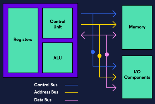
Buses allow us to communicate between different pieces of hardware that work on a system. - Address bus: Holds the address of the instructions in data (like a pointer) - Control bus: Helps synchronize data between every device attached to this bus - Data bus: Handles the transfers of data between attached devices
CPU - Central Processing Unit
The CPU consists of three main components: - Control Unit (CU) - Arithmetic and Logic Unit (ALU) - Registers (Immediate Access Store)
CU - Control Unit
Responsible for: - Controlling and monitoring the input and output of data from the computer’s hardware. - Able to receive and decode instructions and direct operations to other units. - Its primary job is making sure that data is sent to the right component, at the right time, and arrives with integrity. For this it uses what's known as a "Clock".
A high frequency clock
The "Clock" switches between on (1) and off (0), it ticks at a constant rate just like a real clock. The period where the clock has been on and off once is called a cycle. The goal of this is to synchronize between the cpu and the bus (we do something every single tick). - Measured in oscillations per second (1 GHz = 1 billion times per second). - Sends out a regular electrical signal to all components at the same time to coordinate activities.
ALU - Arithmetic and Logic Unit
Carries out logic and arithmetic, completes operations like ADD, AND, OR, NOT, etc. - Arithmetic operations - Logic operations
Registers
Registers are small and limited storages, they are a type of high-speed computer memory that is very close to the CPU. It is the fastest way to store data. - They are fixed in number and size and defined in the Instruction Set Architecture (ISA).
Instruction execution cycle
- The CPU completes a predefined set of steps to execute an instruction. This is called the fetch, decode & execute procedure.
- Fetch an instruction (in memory) from the instruction queue
- Decode the instruction and check for operands
- If operands are involved, fetch the operands from memory / registers
- Execute the instruction and update status flags
- Store the result if required
Reading from memory
- Memory access (RAM) is slower than register access
- Each step takes approximately one clock cycle
- Place the address of the value you want to read on the address bus
- Changes the processor's RD pin (called asserting)
- Wait one clock cycle for memory to respond
-
Copy the data from the data bus to the destination
-
To compare, register access usually takes only one clock cycle
Caching
- To reduce read/write time from memory, caches are used to store data from an address that is consistently being read from or written to. The caches are being constructed by static RAM, which is a special type of RAM that does not need to be refreshed constantly.
Caches: - Level-1 (L1): stored on the CPU - Level-2 (L2): stored outside and accessed by high-speed data bus
Addresses
- Absolute address: a direct reference of specific location.
- Segment address (or offset): starting address of a memory segment with the offset value.